
Comparative Microscopy of Monarch Butterfly Scales
Atomic Force Microscopy (AFM), Scanning Electron Microscopy (SEM), and
optical microscopy are all techniques that analyze and visualize surfaces
and structures at various scales. All three techniques are used to observe
the morphology and structure of samples to better understand physical
properties. Each can provide information about surface morphology at
different scales. While there are many similarities in each technique,
there are significant differences with resolution, depth of field, the type
of information gathered, and physical principles used to collect data.
Applications include material science, biology, and nanotechnology to
characterize properties of materials such as roughness, defects, and
morphology. Looking at the same sample under an AFM, SEM, and Optical
Microscope will provide different types of information as there are different
resolutions and imaging techniques from each instrument.
Butterflies are famous for their iridescent colors, but it is "unusual in how
those colors are produced" (Stone 2015). The wings are "not only colored by
pigments, but also by the scattering of light within micro- and nanoscale lattice
structures" (Stone 2015). This case study uses SEM, AFM, and optical microscopy to
analyze the micro- and nanoscale surface structures of monarch butterfly scales,
highlighting the similarities and differences among these research tools.
Optical Microscope: Keyence VHX-7000
The Keyence VHX-7000 is capable of 4K ultra-high-resolution imaging (20X to 2500X),
achieves a high depth of field, has flexible observation modes, able to stitch
3D and measure, automated functions, and overall, a user-friendly instrument.
The ultra-high-resolution imaging and high depth-of-field allow for precise
analysis and clear images, even on uneven surfaces. Furthermore, it can support
multiple observation methods such as brightfield, darkfield, polarized light,
and differential interference contrast, allowing for a diverse set of needs.
This instrument can obtain surface features, overall morphology, and color
variations.
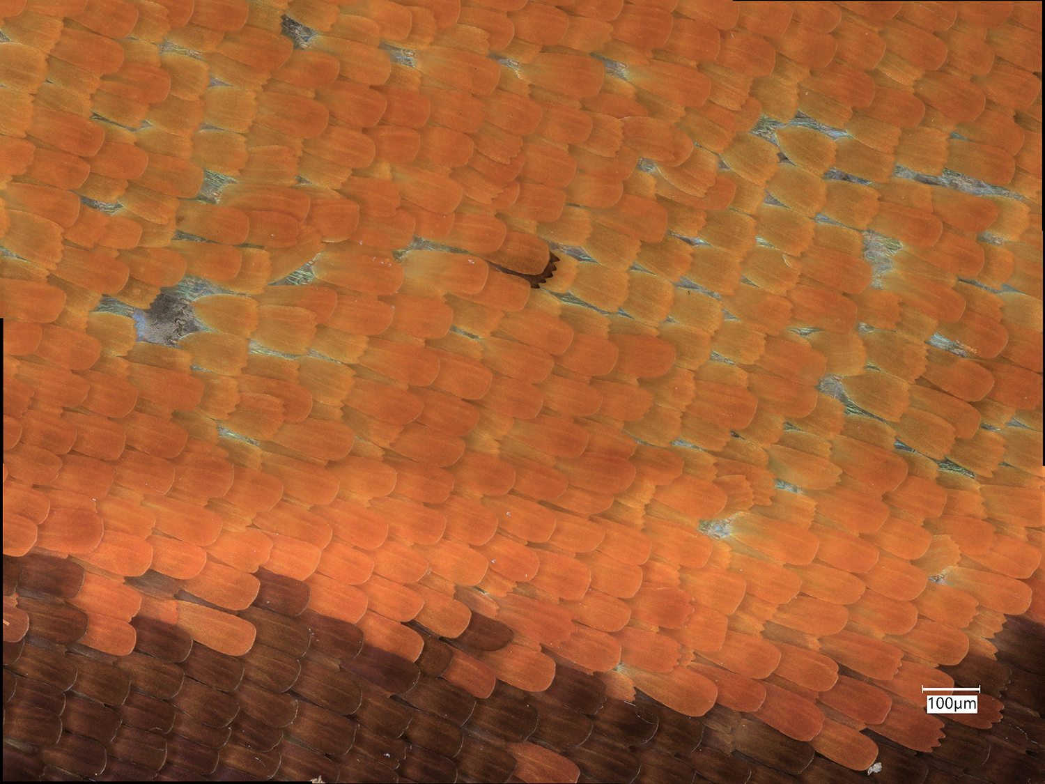
Figure one displays a high-resolution image of a Monarch butterfly wing at ---X.
At this magnification, it is possible to view the surface morphology of the scales,
but not the ridges and cross ribs within an individual scale (Giraldo 2008).
Scanning electron Microscope: JOEL 6500
The JOEL 6500 SEM uses a focused beam of electrons to scan the sample. Based on the
interaction of electrons (backscattered or secondary) with the sample produces signals
to form an image. The SEM is capable of high-resolution imaging (10X to 500,000X)
that can be used to analyze surface morphology as well as conduct elemental analysis.
Even though the images are in grayscale, the magnification is significantly higher
than the optical microscope and can observe nanoscale details.
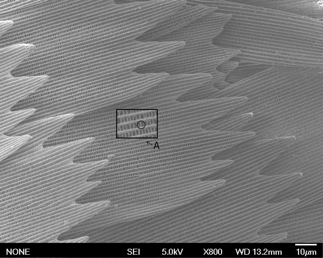
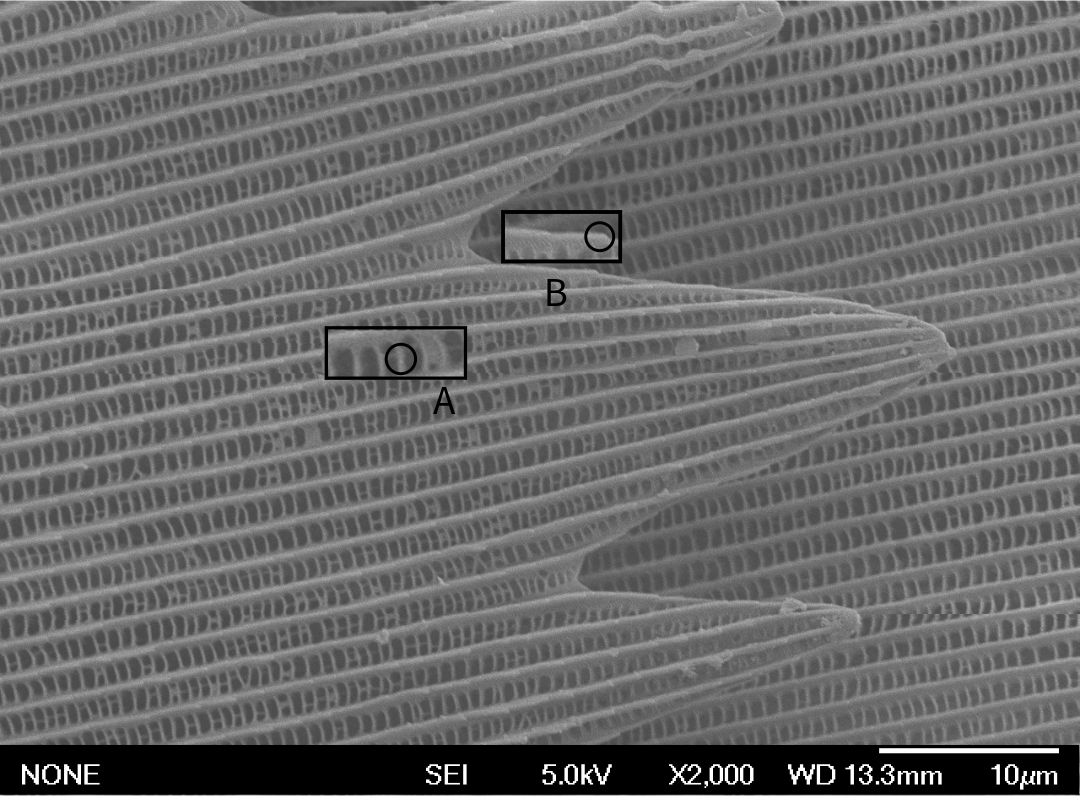
Figure 2 and 3 display nanoscale details of the Monarch butterfly scale at 800X and
2,000X. While both figures display A, the cross ribs of the scale, figure three also
displays the ridges, B.
Applications to SEM: Cryo-SEM
Cryo-scanning electron microscopy (cryo-SEM) rapidly freezes samples and keeps them at
extremely low temperatures for high-resolution surface imaging, preserving their natural
structure. The operating temperature of cryo-EM is usually around -180°C to -196°C. This
technique has numerous applications including tissue and cell development. Other
additional techniques during this process include cryofracture and milling revealing
details about air spaces, water distribution, and subcellular structures.
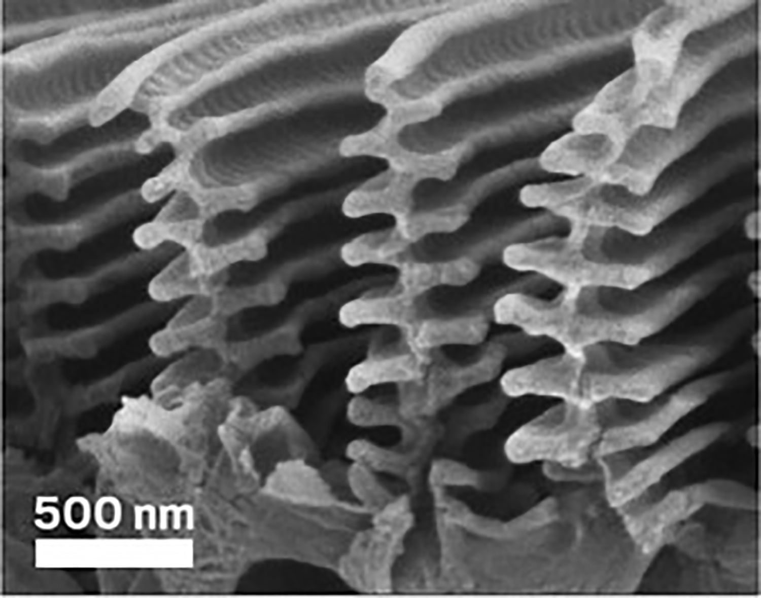
Figure four shows a scanning electron micrograph (SEM) of fractured cross-sections,
revealing the ridges on the upper surface of a butterfly wing scale, which are supported
by underlying structures. These ridges have a layered structure that creates interference,
resulting in the metallic iridescence and sheen characteristic of a butterfly's wing (ACS 2020).
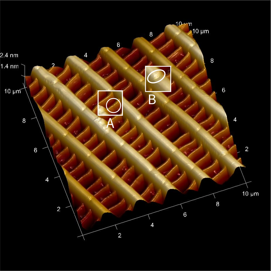
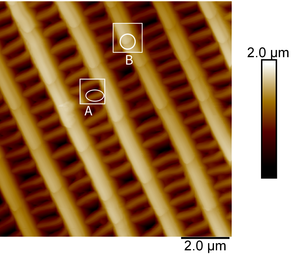
Atomic Force Microscope: Dimension Icon AFM with SanAsyst
Atomic Force Microscopy (AFM) can achieve atomic-level resolution, often less than a nanometer. In this technique, a sharp probe scans the surface of a sample to measure the forces between the tip and the sample, allowing for the creation of detailed 3D surface topography. Applications of AFM include assessing surface roughness, mechanical properties (such as modulus, adhesion, deformation, and force-distance (F-z) curves), electrical properties (including Conductive AFM (CAFM), Kelvin Probe Force Microscopy (KPFM), Electrostatic Force Microscopy (EFM), Tunneling AFM (TUNA), and I-V curves), as well as magnetic properties (Magnetic Force Microscopy (MFM)). AFM is also capable of revealing molecular and atomic-level features, making it a versatile tool in nanotechnology and materials science. Figures 5 and 6 show the 10um morphologies of the Monarch butterfly scale. The height of the cross rib (A) was measured at about 511.25nm and the ridge (B) was measured at about 1.43um.
Conclusions
In conclusion, Atomic Force Microscopy (AFM), Scanning Electron Microscopy (SEM), and optical
microscopy each offer distinct advantages in visualizing and analyzing surfaces and structures
at various scales. These techniques complement one another, providing a comprehensive understanding
of sample morphology and surface characteristics from micro- to nanoscale.
The application of these methods to study the micro- and nanoscale structures of monarch butterfly
wings highlights their unique capabilities and the differences in resolution and imaging techniques.
The butterfly wing is an excellent sample for this comparison due to its intricate and varied surface
features, making it ideal for demonstrating the strengths of each microscopy technique. Utilizing all
three allows for a more complete and detailed characterization of materials, contributing to
advancements in fields like material science, biology, and nanotechnology.
References
Stone, M. (2015, January 22). Understanding butterfly wing color. Penn Today. University of Pennsylvania.
https://penntoday.upenn.edu/2015-01-22/features/understanding-butterfly-wing-color
Giraldo, M. (2008). Butterfly wing scales: Pigmentation and structural properties. Advances in Insect Physiology, 38
American Chemical Society. (2020, July 8). Chemistry in Pictures: Butterfly effect. Chemical & Engineering News.
https://cen.acs.org/materials/photonics/Chemistry-Pictures-Butterfly-effect/98/web/2020/07