Transmission Electron Microscope
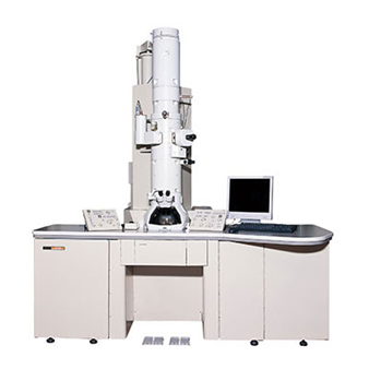
JEOL 2100 200kV TEM
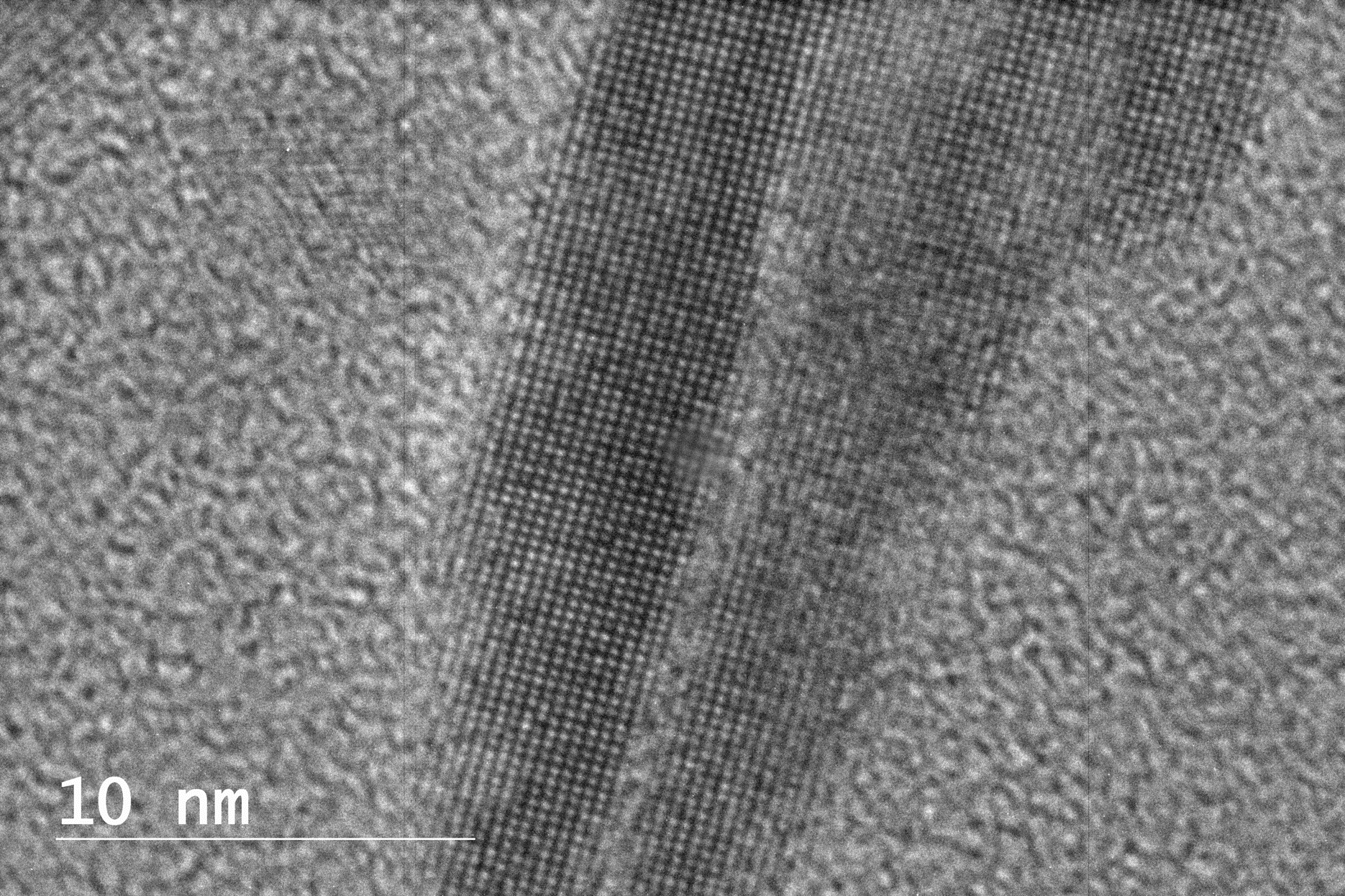
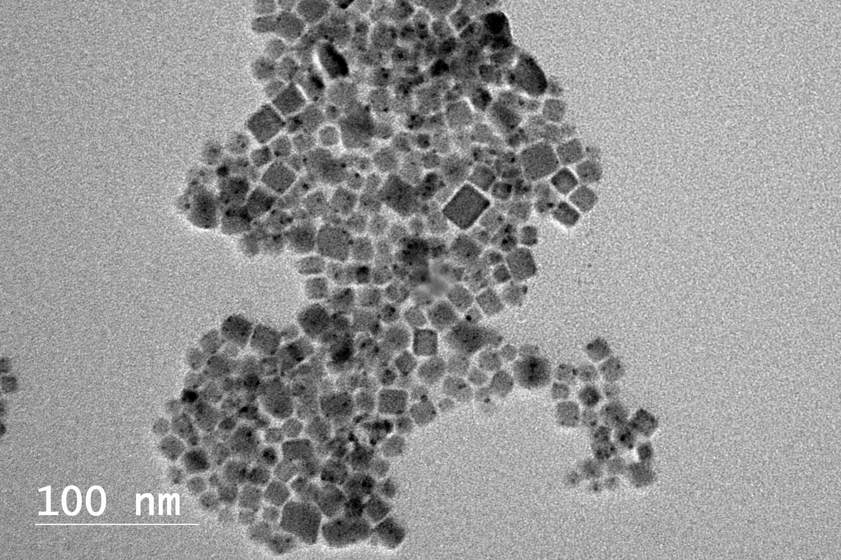
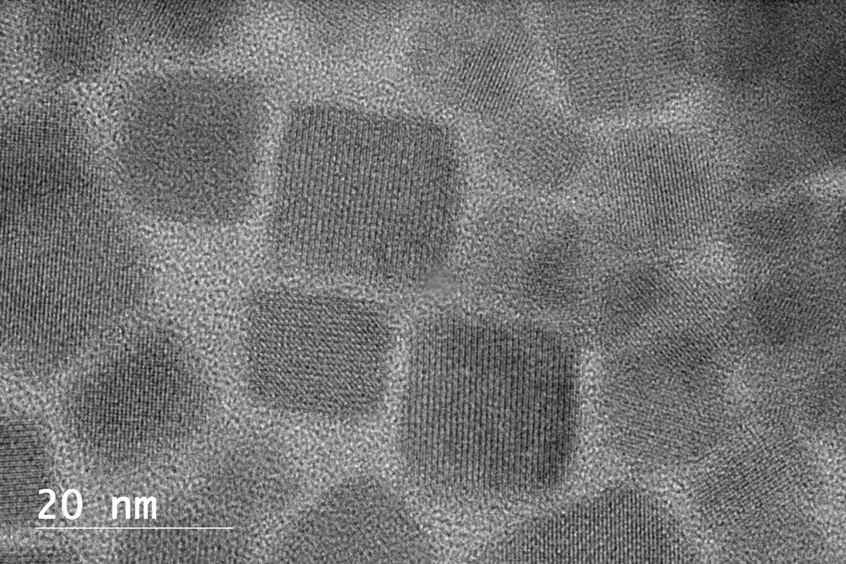
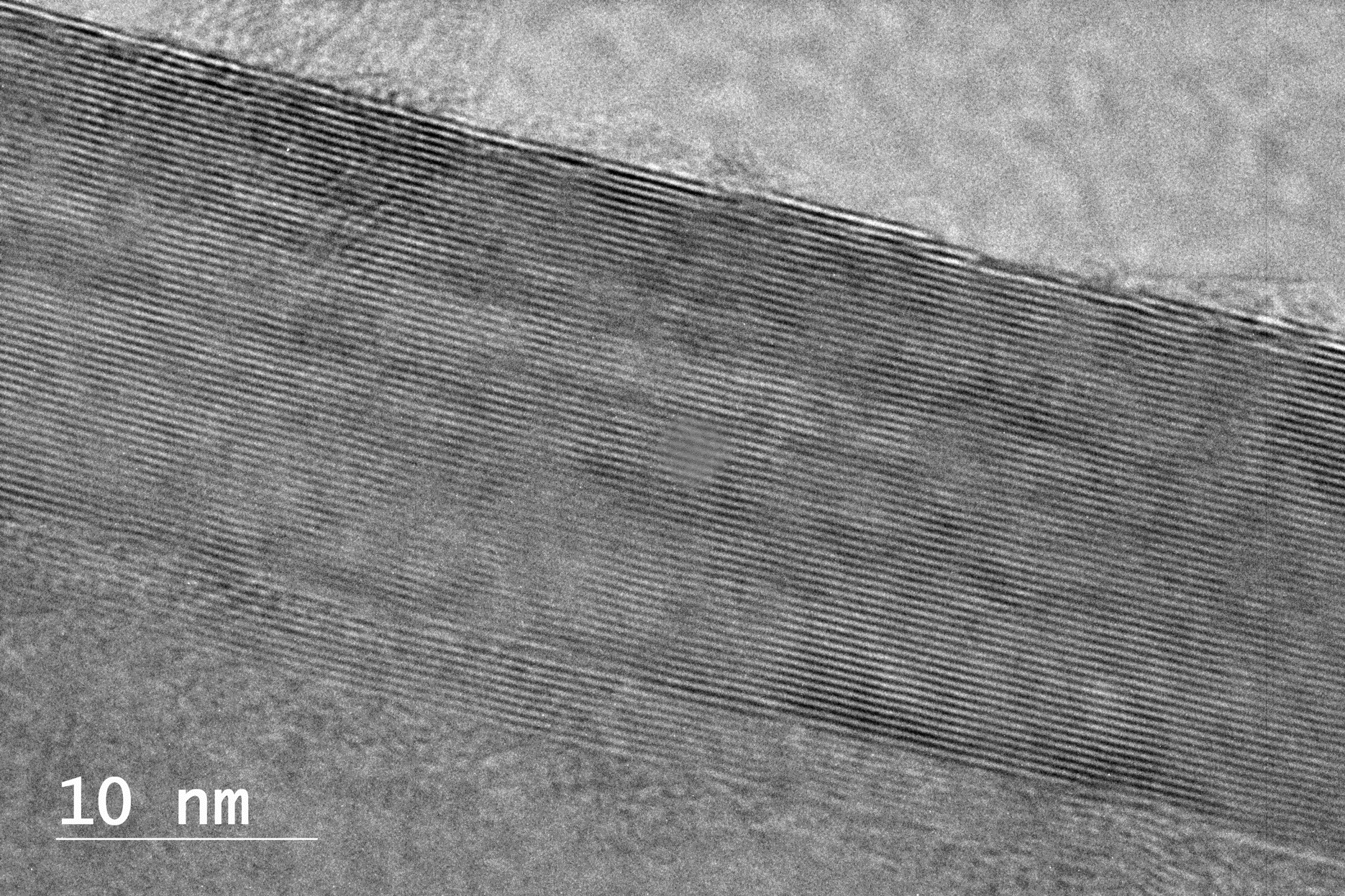
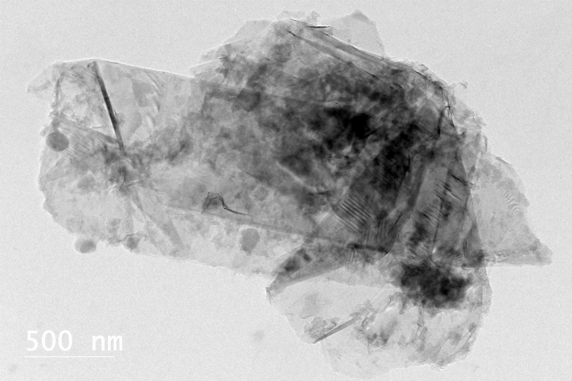
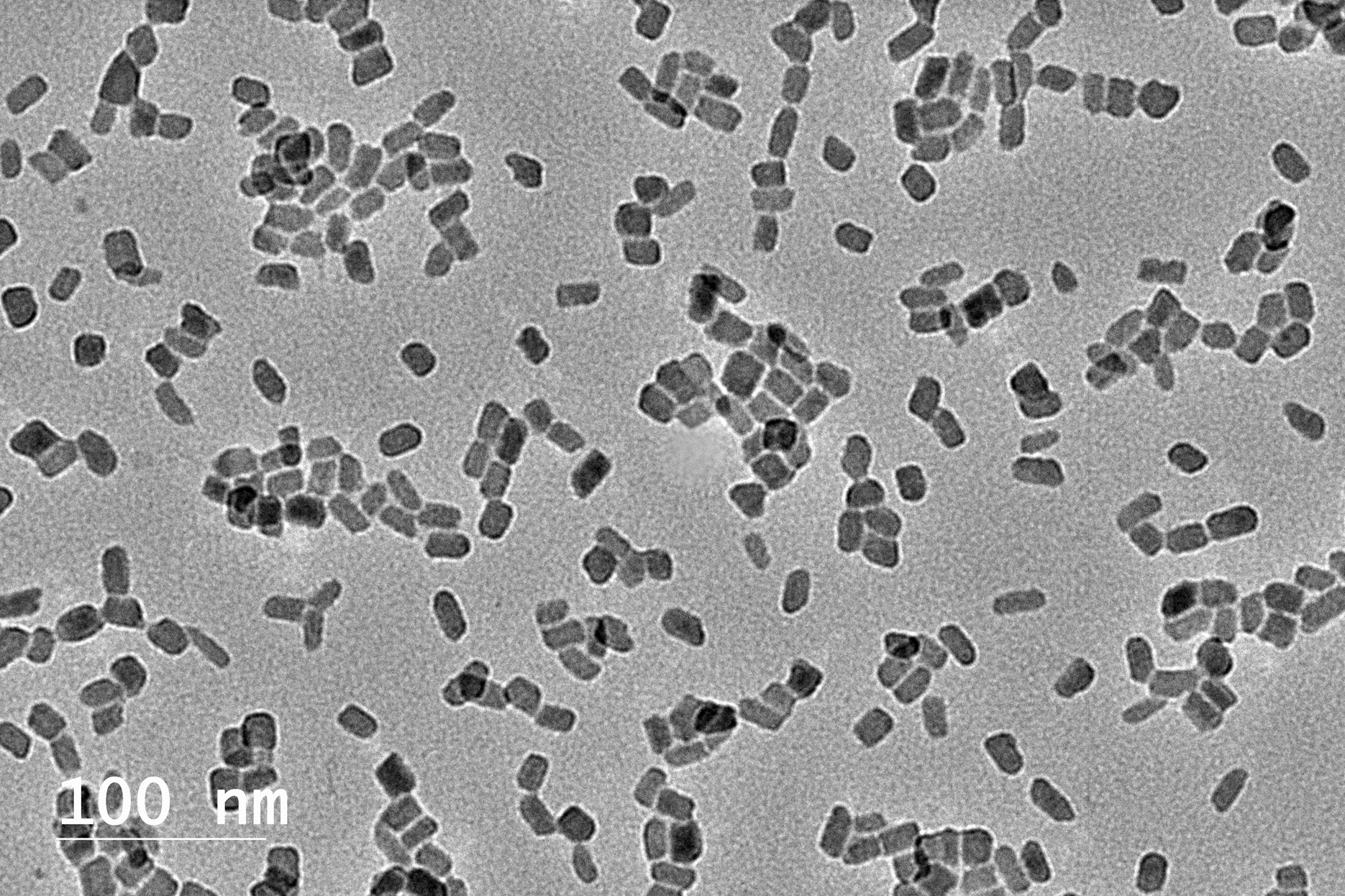
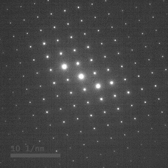
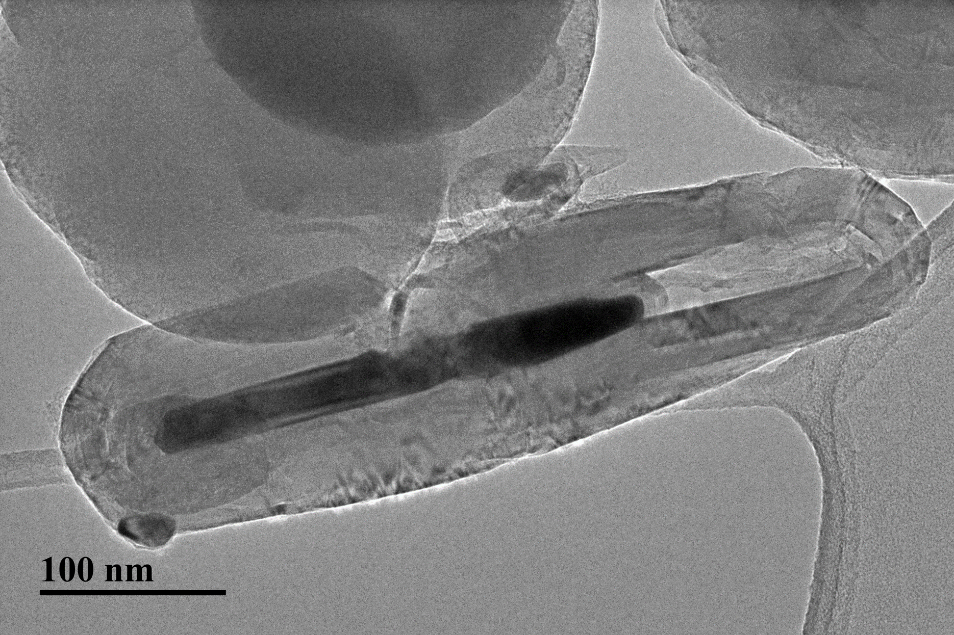
TEM is a type of electron microscope that uses electrons instead of light to magnify a sample at a high resolution which allows the ability to study materials at micro- and nano- scale. This technique uses a beam of electrons transmitted through a specimen to produce an image. The TEM can produce high resolution images as well as other applications including elemental composition, structure resolving, and finding the structure of a crystal.
TEM is a type of electron microscope that uses electrons instead of light to magnify a sample at a high resolution which allows the ability to study materials at micro- and nano- scale. This technique uses a beam of electrons transmitted through a specimen to produce an image. The TEM can produce high resolution images as well as other applications including elemental composition, structure resolving, and finding the structure of a crystal.
Resources:
Specifications:
General Methods Description:
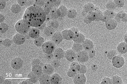
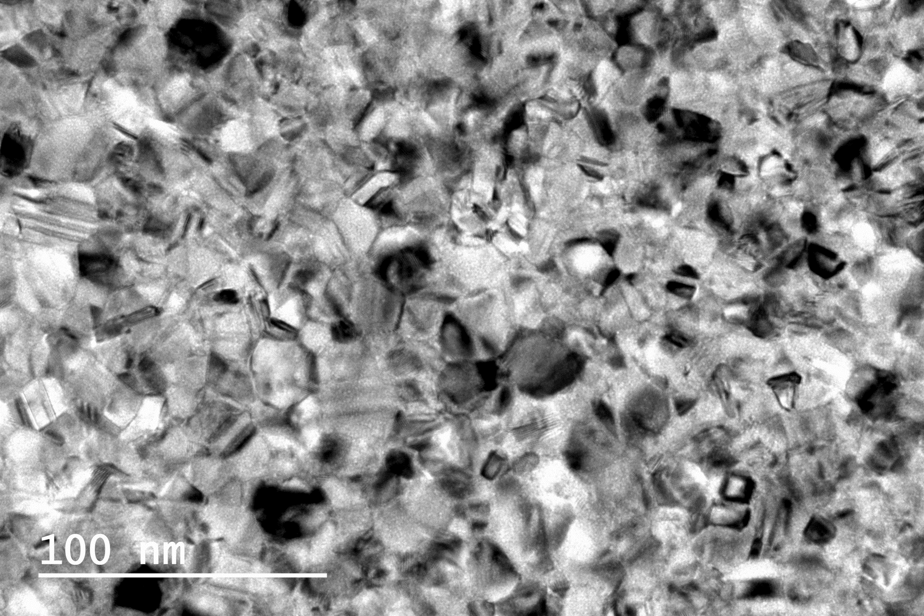
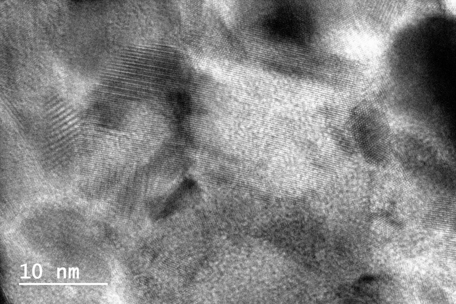
Samples were prepared by drop-casting a dispersion in water or ethanol onto carbon-coated copper grids. Biological samples were stained as needed to enhance contrast. Imaging was performed using a JEOL TEM 2100 operated at 200 kV in bright-field, dark-field, or high-resolution modes. Elemental analysis was conducted using an Oxford X-Max 80 mm EDS detector, acquiring spectra and elemental maps under optimized beam conditions. TEM and EDS data were processed using the manufacturer's software, applying standard background subtraction and peak identification.
Specifications:
| Max Accelerating Voltage | 200 kV |
| Resolution Point | 0.23 nm, Lattice: 0.14 nm |
| Electron Emitter | LaB6 emitter |
| Sample holders | Single Tilt and Low Background double tilt |
| Attachments | - Oxford EDS system for elemental analysis and mapping - Bottom and side mount Gatan Cameras with Digital Micrograph Software |
Samples were prepared by drop-casting a dispersion in water or ethanol onto carbon-coated copper grids. Biological samples were stained as needed to enhance contrast. Imaging was performed using a JEOL TEM 2100 operated at 200 kV in bright-field, dark-field, or high-resolution modes. Elemental analysis was conducted using an Oxford X-Max 80 mm EDS detector, acquiring spectra and elemental maps under optimized beam conditions. TEM and EDS data were processed using the manufacturer's software, applying standard background subtraction and peak identification.